Product Information
Buried layer silicon epitaxial is a silicon monocrystalline thin film with conductive type, resistivity, thickness and lattice structure that is grown on the buried layer semiconductor silicon polished section, which meet the requirements. Compared with conventional semiconductor silicon epitaxial wafers, buried layer epitaxial processes have more precise requirements for the distribution of electrical properties and defect control of epitaxial layers.
 |
Product Parameters Diameter: 200 mm |
Process Introduction
The process of silicon epitaxy of buried layer in semiconductor especially needs to consider the protection of the circuit pattern of buried layer to minimize the influence of distortion and drift caused by epitaxial growth on the circuit pattern of buried layer on the back lithography process.
Relying on the profound accumulation of conventional semiconductor silicon epitaxy technology, the core technology of buried semiconductor silicon epitaxial wafer products developed and manufactured for our customers has reached the domestic leading and international advanced level, and the technology level can be comparable to the international first-class semiconductor manufacturers. The technical research and development department of Shanghai Shanghai Wafer Works Corporation has controlled the temperature field uniformity of the epitaxial furnace through a special process, solved various problems of buried layer silicon epitaxy such as chip surface graphic drift and self-doping, and developed high-quality buried layer epitaxy products to fill the gap of this technology in the country.
Since the buried layer epitaxial technology needs to be integrated into the complete process flow of the customer's chip manufacturing, the customer's requirements on the quality control, production environment, system management and control of the buried layer epitaxial technology are consistent with its own requirements. We are the international first-tier chip manufacturers for mass OEM buried layer epitaxy for many years, the technology level has reached the level of the international first-tier semiconductor chip manufacturers, highly recognized by customers, is the most domestic supplier of buried layer epitaxial products.
The manufacturing process includes epitaxial growth, epitaxial wafer cleaning, epitaxial wafer testing and packaging.
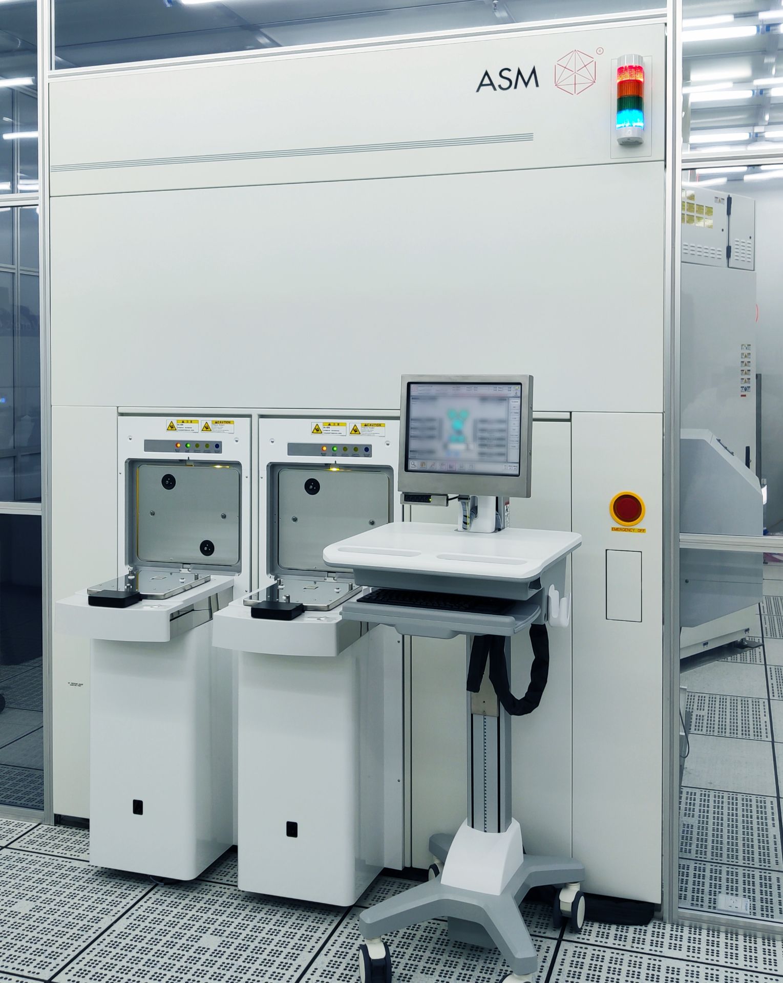 |
Epitaxial growth Use chemical vapor deposition on the polished section specified thickness of layer or one multilayer growth of single crystal layer, through the incorporation of P type boron or N type phosphorus gas to control the resistivity, and use the reaction temperature, the extension of temperature gradient on the edge of the gas flow velocity, center and process adjustment, to adjust the resistivity and thickness uniformity, transition zone width, grain, defect (fault, slip line, fog, etc.) the effective control of key parameters, such as, realizes the optimal quality of the epitaxial layer and meet the requirements of customer manufacturing process. |
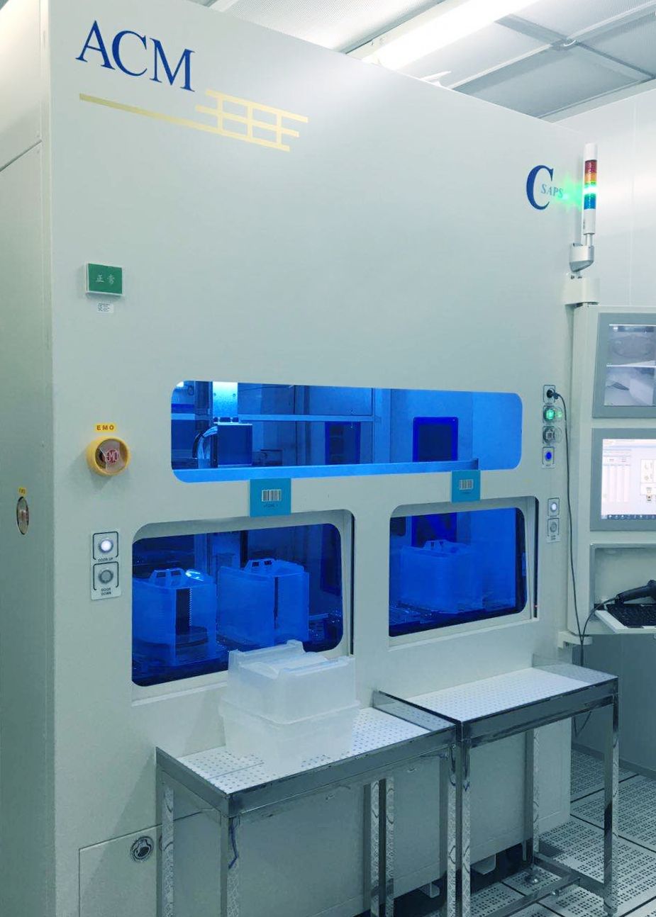 |
Epitaxial wafer cleaning The final cleaning of silicon wafer is carried out using THE RCA process. The purpose is to remove various contaminants on the surface of silicon wafer, such as surface dust particles, organic matter, metals, and other possible |
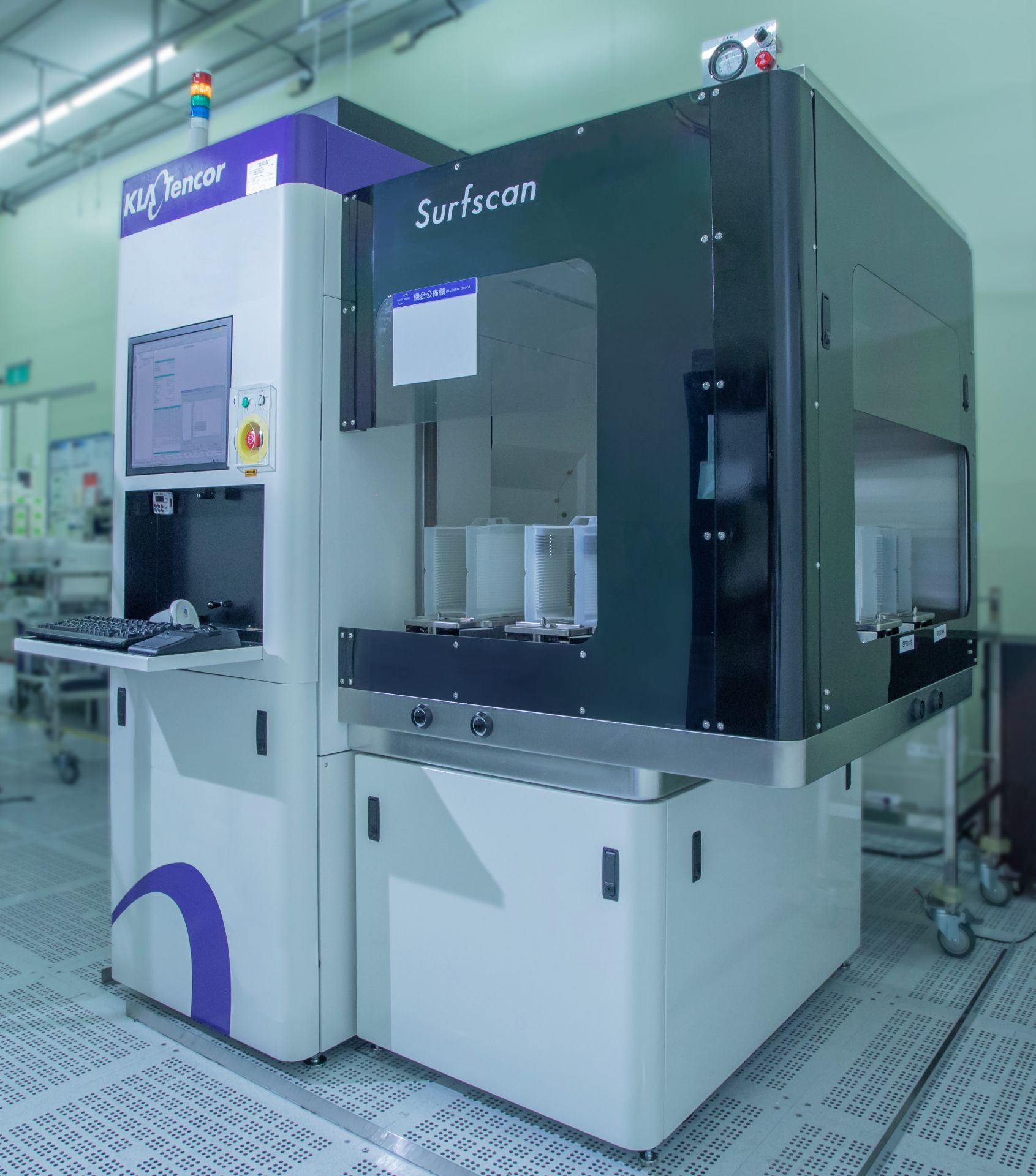 |
Epitaxial wafer detection The epitaxial wafer is cleaned by measuring its physical characteristics such as resistivity, thickness, flatness and warpness with equipment, and then the surface dust particles, organic matter, metal and other defects are detected with high-precision equipment to ensure that the quality of epitaxial layer meets customers' requirements. |
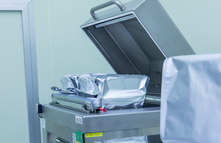 |
Packing After containing silicon wafer in silicon wafer box, PE bag and aluminum foil bag are covered in the packing process, so that the quality will not be damaged by environment, external force and other factors during storage and transportation. |
Product Application
Buried layer epitaxy can effectively reduce series resistance, simplify isolation technology and improve device performance; therefore, it is widely used in power Management IC (PMIC) chip manufacturing and other special process platform.