Product Information
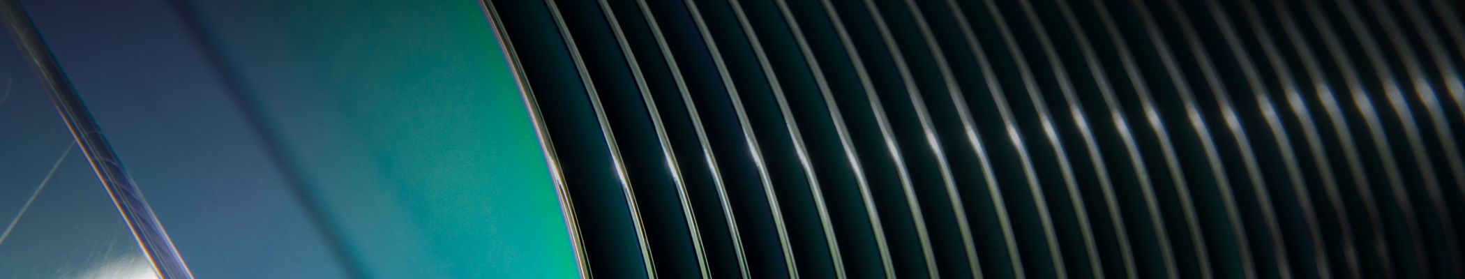
Epitaxy is a new silicon single crystal layer that grows one or more layers on the polish section by chemical vapor deposition, and the product parameters such as doping type, resistivity, thickness and lattice structure, etc., which all meet the requirements of specific devices, with excellent uniformity and extremely low defect density.
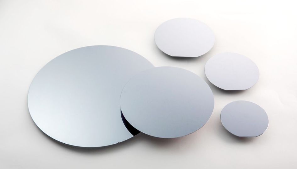 |
Product Parameters Diameter: 150/200/300 mm |
Process Introduction
The products have excellent competitiveness, and Wafer Works Corporation is one of the few domestic semiconductor silicon epitaxial wafer manufacturers with full process production capacity from crystal growth, silicon wafer molding to epitaxial growth.With rich production experience in each manufacturing process, as well as fine quality control ability in the production process, “Wafer Works” tailor-makes integrated customized silicon epitaxial wafers for customers, realizing effective matching of epitaxial layer and substrate geometry, and achieving integrated silicon epitaxial wafers of different specifications.
The manufacturing process includes epitaxial growth, epitaxial wafer cleaning, epitaxial wafer testing and packaging.
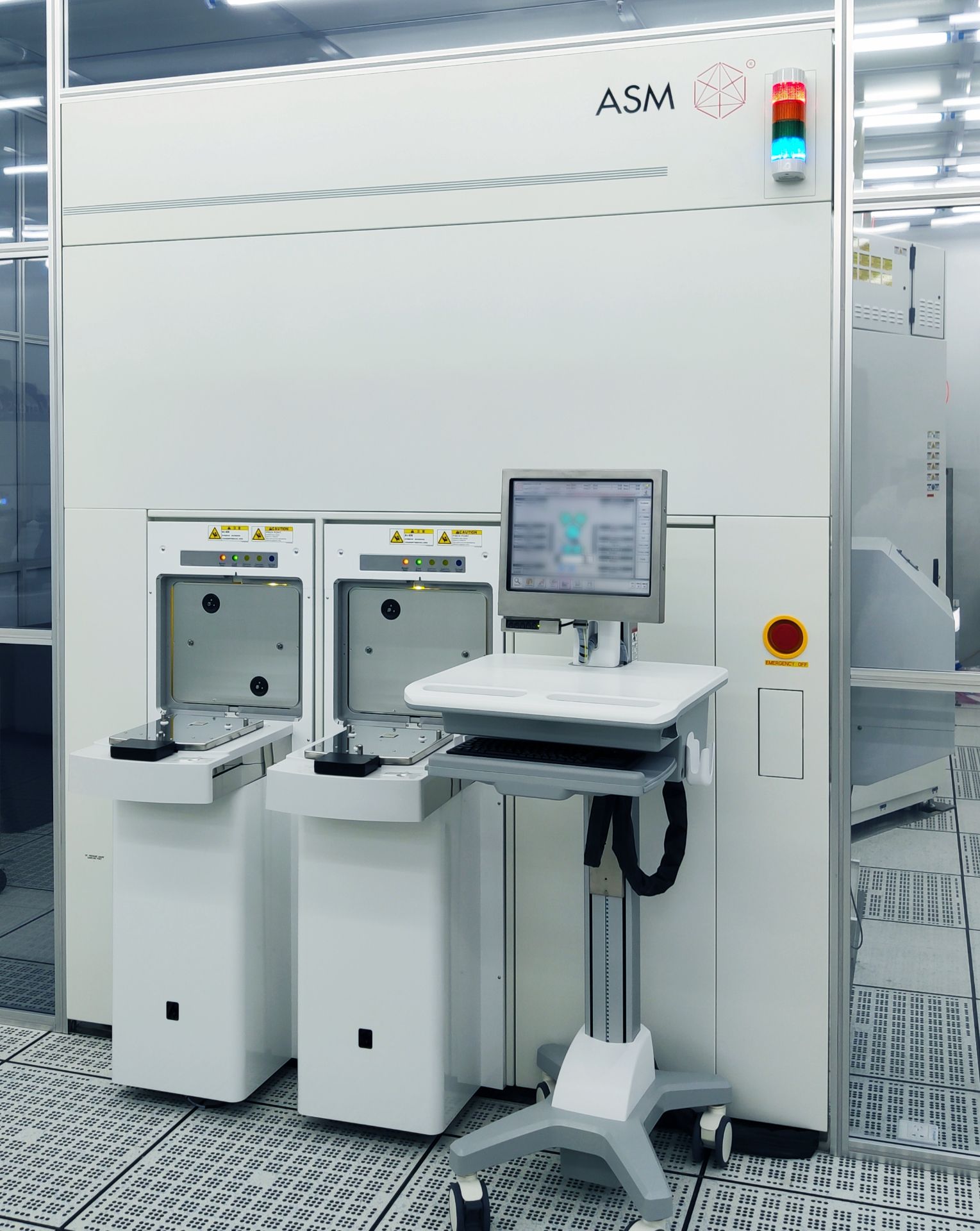 |
Epitaxial growth Use chemical vapor deposition on the polished section specified thickness of layer or one multilayer growth of single crystal layer, through the incorporation of P type boron or N type phosphorus gas to control the resistivity, and use the reaction temperature, the extension of temperature gradient on the edge of the gas flow velocity, center and process adjustment, to adjust the resistivity and thickness uniformity, transition zone width, grain, defect (fault, slip line, fog, etc.) the effective control of key parameters, such as, realizes the optimal quality of the epitaxial layer and meet the requirements of customer manufacturing process. |
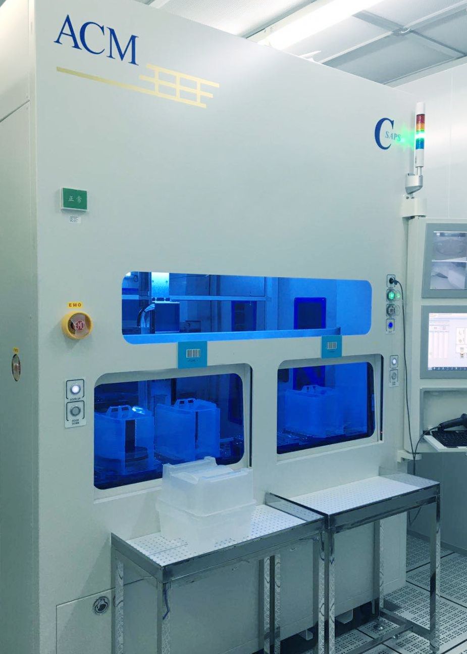 |
Epitaxial wafer cleaning The final cleaning of silicon wafer is carried out using THE RCA process. The purpose is to remove various contaminants on the surface of silicon wafer, such as surface dust particles, organic matter, metals, and other possible |
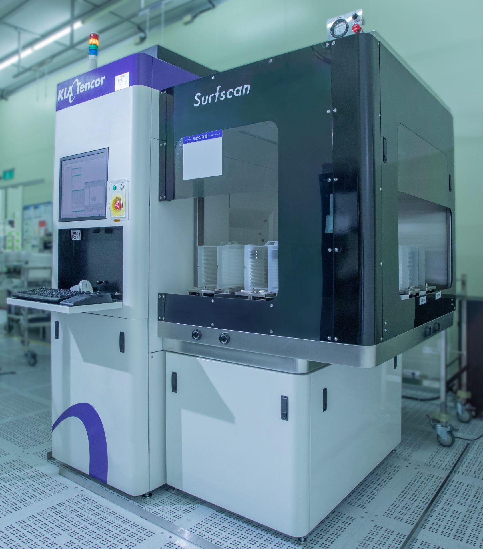 |
Epitaxial wafer detection The epitaxial wafer is cleaned by measuring its physical characteristics such as resistivity, thickness, flatness and warpness with equipment, and then the surface dust particles, organic matter, metal and other defects are detected with high-precision equipment to ensure that the quality of epitaxial layer meets customers' requirements. |
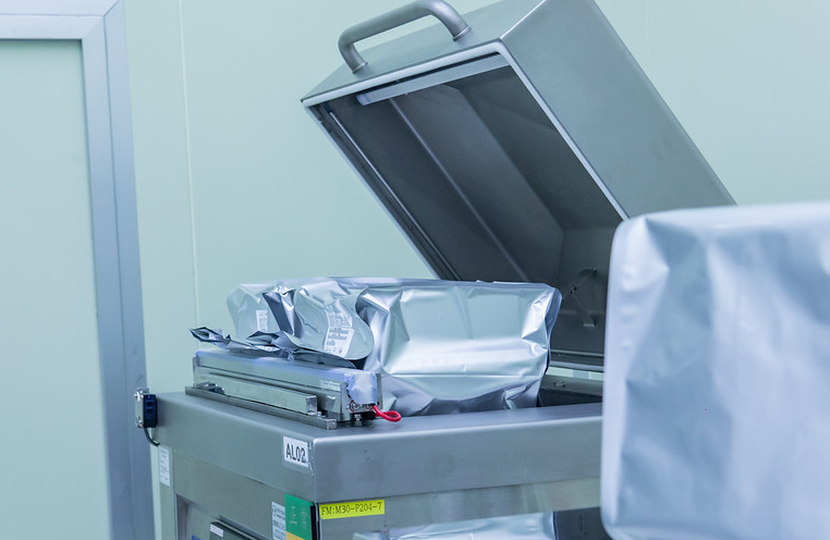 |
Packing After containing silicon wafer in silicon wafer box, PE bag and aluminum foil bag are covered in the packing process, so that the quality will not be damaged by environment, external force and other factors during storage and transportation. |
Product Application
Our silicon epitaxial wafer is characterized by high voltage resistance and low on-resistance, which enables the device manufactured by the customer to operate in a highly stable state. It is mainly used for preparing MOSFET, (Insulated Gate Bipolar Transistor (IGBT), Power devices such as transistors and CMOS image sensor (CIS), power management IC (PMIC), integrated circuit and other chips. It is widely used in automobile, communication, electric power, industry, consumer electronics, high-end equipment and other fields.