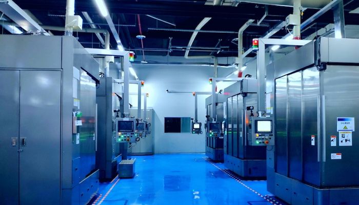
Product Information
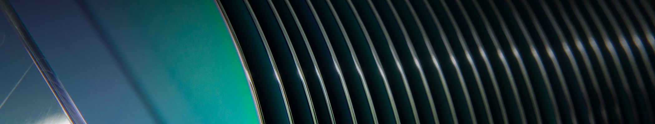
The reason why the semiconductor silicon epitaxial wafers of Wafer Works (Shanghai) Corporation are widely recognized by customers at home and abroad with the world's leading market share is mainly because of the integrated production of the products and the mastery of crystal growth, silicon wafer molding and epitaxial growth, the three major technologies, which complement and reinforce each other to achieve the highest epitaxial quality. The technology of polished section has a huge impact on the Company’s competitiveness.
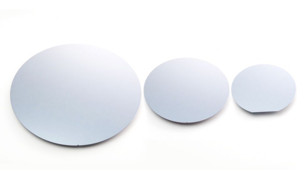 |
Product Parameters Diameter: 150/200 mm |
Process Introduction
Polished section is mainly divided into two key processes, crystal growth technology and silicon wafer molding technology.
|
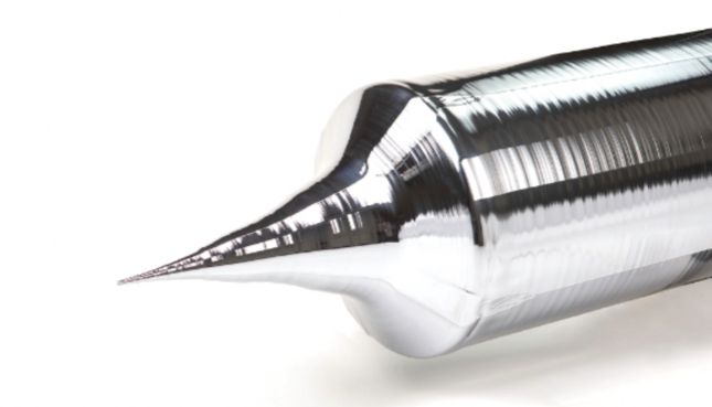
Crystal Growth Technology The focus of single crystal growth technology is to ensure that the drawn ingots can effectively control the density of crystal defects while maintaining a very high level of purity, thus reducing the number of defects in the wafers made from them. For a long time, only a few silicon wafer manufacturers in Japan, Europe and the United States have the technical ability to produce ultra-low defect single crystal silicon rod, while Shanghai Wafer Works Corporation is one of the few domestic manufacturers that can independently develop ultra-low defect single crystal silicon rod growth technology.
We use CZ method to carry on the wafer (100) and (111) single crystal growth, mixed with P type boron atoms or N type phosphorus, arsenic, antimony atoms to control the resistivity, combined with perfect long crystal thermal field system, integrated with the specific process, pressure, flow, temperature to adjust RRG, oxygen content, ORG, micro defects, such as related parameters, to meet customer demand, to realize ultra-low resistance is the growth of the crystal rods, and reduce the conduction resistance value of power component. It is also one of the most important contributions to the use of heavily doped substrate epitaxial wafers. |
 |
|
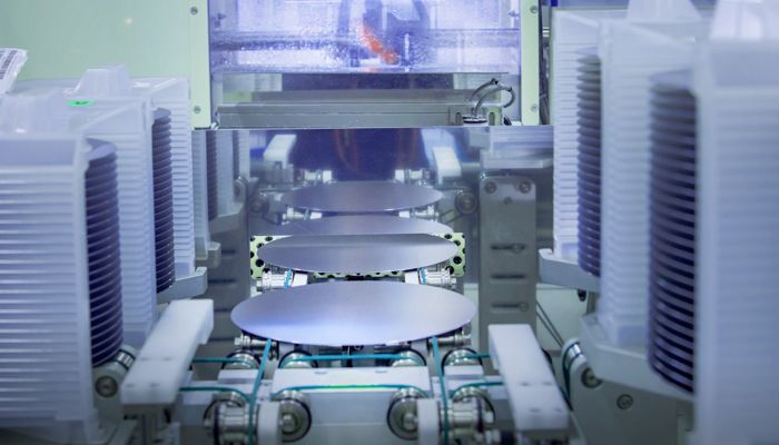
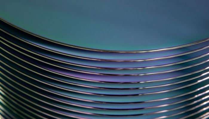
Silicon Wafer Molding Technology Silicon wafer is the basis of semiconductor components, and its quality has a decisive influence on the construction of semiconductor devices. Wafer processing mainly includes wafer slicing, wafer chamfering, wafer grinding, wafer corrosion, wafer back processing, wafer polishing, wafer cleaning, wafer detection and packaging, etc. |
 |
 |
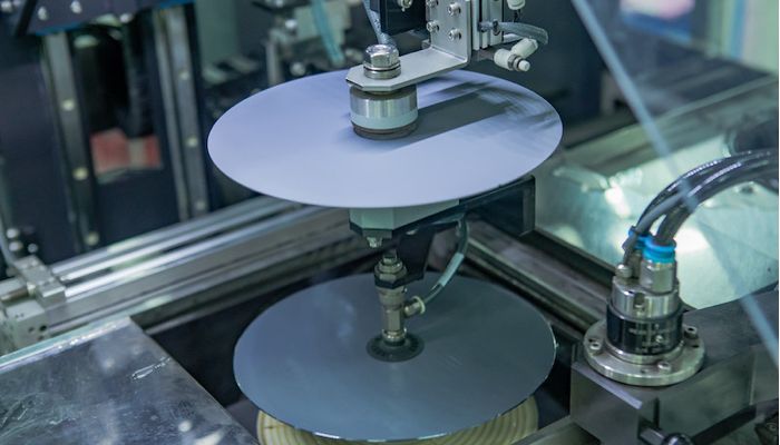
Crystal bar slicing The crystal bar is cut into silicon wafers with precise geometric dimensions by a cutting machine, and the warping degree and stress distribution of silicon wafers are controlled by adjusting relevant parameters of the machine. |
 |
Silicon wafer chamfering After the wafer is sliced, the edges usually have acute angles and minor damage. This process can effectively remove the wafer edge damage and achieve a degree of refinement. Suitable chamfering can help eliminate the possibility of future polished section or epitaxial wafer damage during the circuit manufacturing process. |
 |
Silicon wafer grinding It is a key process that affects the warpage, flatness and thickness uniformity of wafer products. The slicing process can cause surface damage, so the process is used to remove the damaged layer. |
 |
Corrosion of silicon wafer After slicing and grinding, the surface of silicon wafer will form a layer of damage due to machining stress. The etching process is to remove the surface damage layer by chemical reaction with appropriate acidic or alkaline solution in a precise temperature control range. |
 |
Crystalback processing Crystalback processing consists of three processes: sandblasting, polysilicon film and silicon dioxide film. The three crystalback processing processes can be combined according to different requirements. Among them, sandblasting and polysilicon film have external impurity absorption effect. |
 |
Crystalback processing Crystalback processing consists of three processes: sandblasting, polysilicon film and silicon dioxide film. The three crystalback processing processes can be combined according to different requirements.Among them, silica can inhibit the self-doping effect during epitaxial growth. |
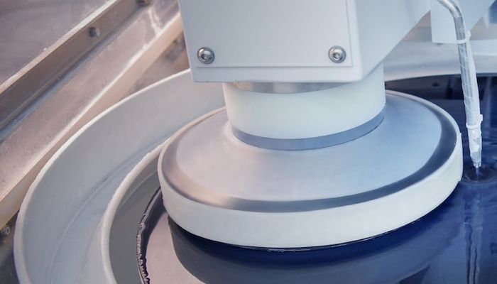 |
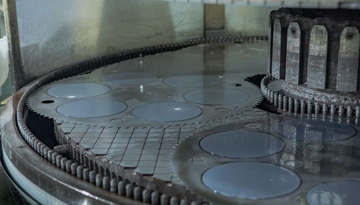
Silicon wafer polishing The etching surface of the wafer is smoothed into nano-level by chemical mechanical grinding, and the indexes such as warping degree and flatness degree of silicon wafer are taken into consideration to avoid problems encountered in microlithography process of silicon wafer in high-end applications. |
 |
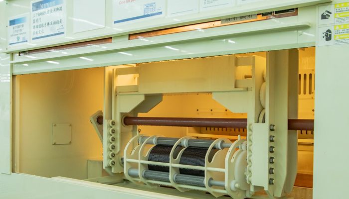
Silicon wafer cleaning The RCA process is used for the final cleaning of silicon wafer. The purpose is to remove various contaminants on the surface of silicon wafer, such as surface dust particles, organic matter, metal and other possible contamination. |
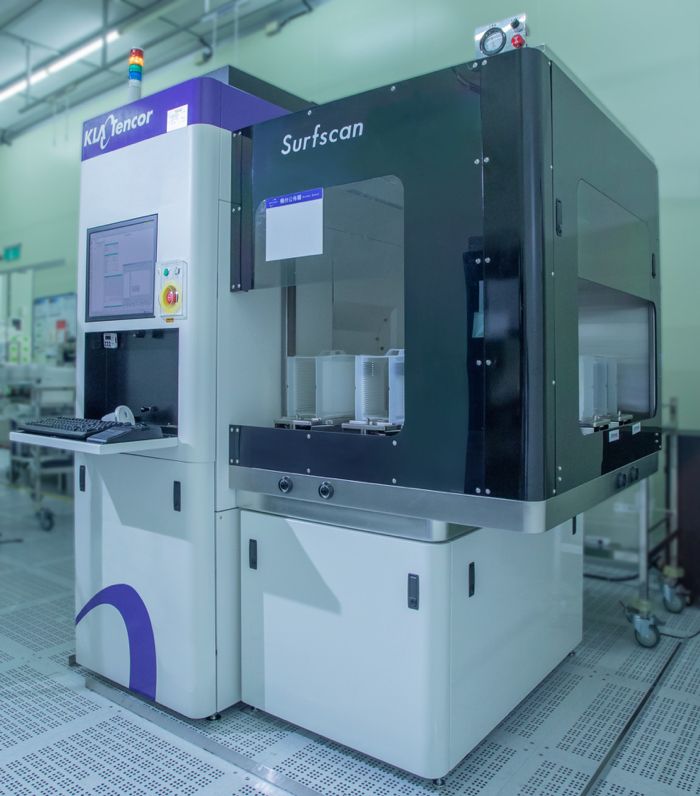 |
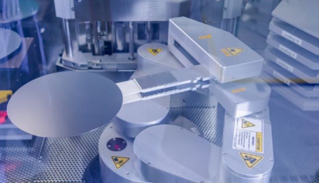
Silicon wafer detection the silicon wafer is cleaned by measuring its physical characteristics such as resistivity, thickness, flatness and warping degree with the equipment, and then the surface dust particles, organic matter, metal and other defects are detected with the equipment of high precision density to ensure the quality of the silicon wafer meets customers' requirements. (The model will be replaced) |
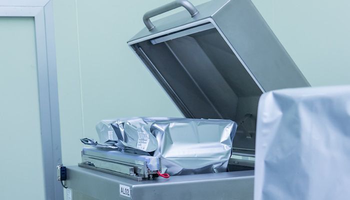 |
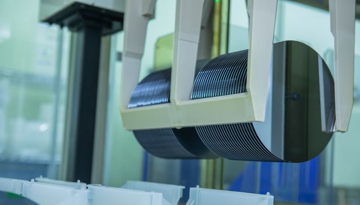
Packing After containing silicon wafer in silicon wafer box, PE bag and aluminum foil bag are covered in the packing process, so that the quality will not be damaged by environment, external force and other factors during storage and transportation. |
Product Application
According to different doping amount, lightly doped polishes are mainly used for manufacturing logic IC, power management IC and other products, while heavily doped polished sections are mostly used for epitaxial technology substrate.